Analysis of semiconductor target
Analysis of semiconductor target
In today's and future semiconductor manufacturing processes, sputtering target is undoubtedly the most important raw material, and its quality and purity play a key role in the subsequent production quality of the semiconductor industry chain.
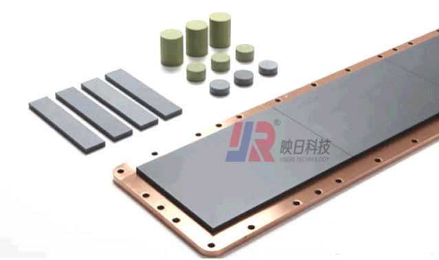
Targets, especially high-purity sputtering targets, are used in the physical vapor deposition (PVD) process for the manufacture of electronic components. They are the key materials for the preparation of surface electronic films such as wafers, panels and solar cells.
Sputtering is not only the main technology for preparing thin film materials, but also a kind of PVD. By bombarding the target with ions in PVD equipment, the metal atoms in the target escape with a certain energy, so as to deposit and splash metal films on the wafer surface. The bombarded solid is the raw material for depositing films by sputtering method, which is called sputtering target.
Compared with another PVD process - vacuum coating, the sputtering coating process has good repeatability and controllable film thickness, and can obtain films with uniform thickness on a large area of substrate materials. The prepared films have the advantages of high purity, good compactness and strong adhesion with substrate materials. They have become the main technology for preparing film materials.